Lab 4 : Video Graphics Array and Image Buffer
Introduction
The Video Graphics Array (VGA) protocol is a simple
protocol for displaying graphics to a CRT and/or most LCD computer
displays. The protocol involves "scanning" the screen and using
two signals called hsync and vsync to synchronize
the exact location on the screen where cursor is ready to draw.
The user guide shows the technical specifics of how the signals
are generated for the VGA protocol. You will have to read the Xilinx
Spartan-3E user guide pages to be more familiar with what you are
working with for this lab. VGA timing information can be found at
VGA Timing and a VGA resolution calculator can be found at
VGA to
RGB.
The FPGA board comes with a standard VGA connector and use five
signals to communicate with the display. The signals are hsync,
vsync, red, green, and blue. With these three signals,
we can successfully generate eight different colors, which is admittedly
somewhat limiting, but useful for instructional purposes.
A VGA Driver is typically nothing more than some logic that drives
horizontal and vertical sync signals on and off so the scan gun
behind your monitor knows when to start shooting the next row or
column.
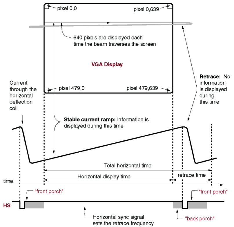
Figure: Shows the timing diagram of hsync.
The timing table for the horizontal sync is shown in the figure
below (you will see later that the vertical sync works exactly the
same).
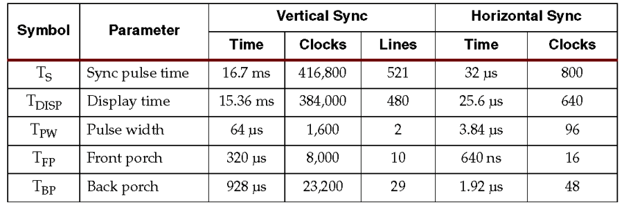
Figure: Shows the timing table for hsync.
At the start of a line, the horizontal sync signal drops to a logical
low for a certain amount of time. The horizontal sync signal then
gets pulsed to a logical high, but at this point, the VGA scan gun
is not ready to draw onto the screen; this is called the front porch.
After a specified front porch period, the screen is ready to display
onto the screen. The horizontal sync allows for 640 distinct pixels
to be displayed before going into the back porch stage. In the back
porch stage, the VGA scan gun has actually passed the viewable portion
of the screen, and cannot paint to the screen. Finally, the pulse
is dropped again, and the process is repeated.
Your first (and most difficult) task will be to capture the VGA
Driver behavior as sequential logic. Before we go into details,
shown below is a block diagram of the VGA Driver component you will
be designing. The inputs into the VGA Driver will be a clock and
reset. The clock will be operating at 25 MHz, but as we learned
in the previous lab, we can assume that we can input an exact 25MHz
clock using the clock generator or DCM component. The outputs from
your VGA driver will be a hsync and vsync signals. These are single
bit values. The last two outputs will hcount and vcount. hcount
will be N bits wide, since we need to be able to count to at least
800 for an entire row of display information. Similarly, vcount
will be N bits. Both hsync and vsync, you need to be able to implement
timing diagram in figure below.
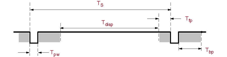
Figure: Shows the timing diagram for hsync and vsync.
You'll notice several different widths specified for this timing
diagram:
- Tpw: Time of the pulse width: How long to keep the signal
low
- Ts : Time period: One complete row/column of information
- Tdisp : Time of Display: This is the time we can actually
display information
- Tfp: Time front porch: The amount of time for the front
porch
- Tbp: Time back porch: The amount of time for the back porch
Both the horizontal and vertical sync signals capture the same timing
model, the only difference being the lengths of each of the pulse
width, front porch, back porch, display time, etc. You can find
the exact timings for each signal in the Spartan 3E Users Manual.
You will also need to maintain counters for both the vertical and
horizontal count, because these are what actually allow other components
to display information at the correct time. For instance, if your
VGA driver gave an hcount = 500, and vcount = 400, another component
could color that appropriate pixel.
So how do we actually model this component using the techniques
you have learned in class? Well, first you need to decide whether
you can capture the behavior with a HLSM, FSM, or combinational
logic. Can the VGA display be captured with one state machine, multiple
state machines? What's easier? This lab will be the first where
you basically need to make all the design decisions. The hardest
part of this lab will be coming up with design on paper. Translating
your design to VHDL will be the easy part.
Note: VGA pixels must be set to black outside the coloring region, if you fail to do so the driver may not work.
Part 1 - Design a Synchronous Counters
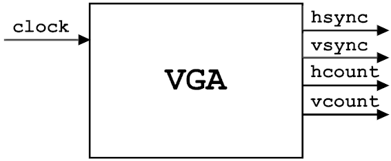
Figure: Shows a high-level view of the first VGA driver to create.
Inputs: Clock, Reset, Enable
Outputs: Hsync, Vsync, Hcount, Vcount
Note: Timing for 640 by 480 VGA display. The horizontal
counter is the fast counter and the vertical counter is the slower
counter.
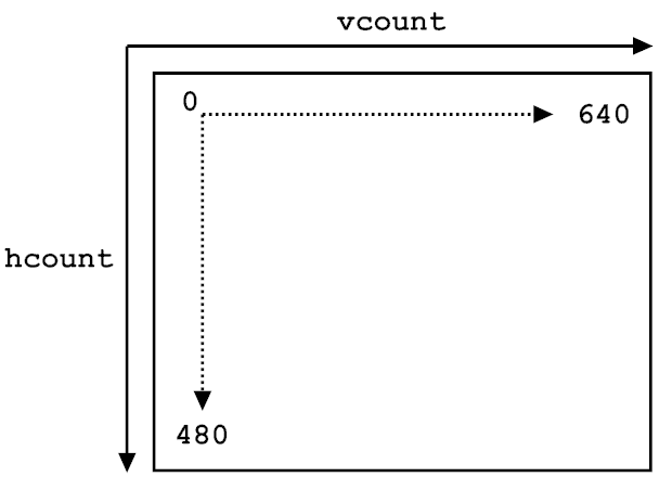
Figure: Shows how hcount and vcount correspond to the screen.
For this lab, you will allow several methods: behavioral by FSM
or structural using counters and a datapath.
Method 1: Single Behavioral FSM
Constants for Horizontal Synchronization
- H_PIXELS = 640
- H_SYNC_PULSE_WIDTH = 96
- H_FRONT_PORCH_WIDTH = 16
- H_BACK_PORCH_WIDTH = 48
- H_POLARITY = 0
Note:
The horizontal increment increases by one when is exclusively
less than (H_PIXELS + H_FRONT_PORCH_WIDTH + H_SYNC_PULSE_WIDTH
+ H_BACK_PORCH_WIDTH), otherwise reset to zero.
The horizontal sync should be low when (horizontal increment
is exclusively less than H_PIXELS + H_FRONT_PORCH_WIDTH + H_SYNC_PULSE_WIDTH)
and (horizontal increment is greater than or equal to H_PIXELS
+ H_FRONT_PORCH_WIDTH), when others it is high.
Constants for Vertical Synchronization
- V_PIXELS = 480
- V_SYNC_PULSE_WIDTH = 2
- V_FRONT_PORCH_WIDTH = 11
- V_BACK_PORCH_WIDTH = 31
- V_POLARITY = 0
Note: The vertical increment increases by one
when the horizontal increment reset to zero and vertical
increment is exclusively less than (V_PIXELS + V_FRONT_PORCH_WIDTH
+ V_SYNC_PULSE_WIDTH + V_BACK_PORCH_WIDTH), otherwise reset
to zero.
The vertival sync should be low when (vertical increment
is exclusively less or equal than H_PIXELS + H_FRONT_PORCH_WIDTH
+ H_SYNC_PULSE_WIDTH) and (vertical increment is greater than
or equal to H_PIXELS + H_FRONT_PORCH_WIDTH), when others it
is high.
Method 2: Mini-Timer Circuits
VGA protocol in VHDL is simply a timer circuit with an FSM. In fact,
you should have implement the VGA protocol in lab 1. The output
of the faster running timer is for hsync and the one of the slower
running timer is for vsync. The counter value from the faster running
timer when valid signal is high is the double of the horizontal
position inside the display time (the counter counts up to 1280),
and the counter from the slower running timer is for vertical. To
make the counter from the faster timer represents the horizontal
position, we can divide the counter by 2 (which is simply ignore
the last bit of the counter).
If you designed the VGA protocol correctly in lab 1, the remaining
step is to create a second syncfsm. Remember in syncfsm, we had
{96, 48, 640, 16} each minus one; in syncfsm2, you will use {2,
33, 480, 10} each minus one. The reasoning for this is because we
want the next state at the values not lagging behind by one. It
is recommended to start using generics when you can because the
generality allows for portability and core re-use.
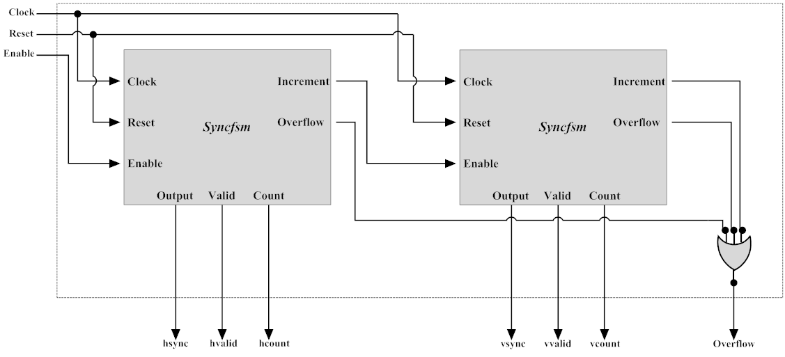
Figure: Shows block diagram of VGA driver using Mini-Timer Circuits.
The only important outputs for this diagram are hsync, hcount,
vsync, and vcount; the others can be discarded by port mapping
them to open in VHDL.
When Completed
A test bench check is not required, however it would if you design
a test bench to test your VGA syncs operate correctly before you.
If you ask the TA later on during the download phase why your VGA
component isn't working, we will first ask to see your test bench
to verify you have the correct behavior. Here is a sample test bench:
vga_tb.vhdl
Part 2 - TV Bars
Figure: TV bars
The next part of the lab will be simulate colored bars
on your VGA monitor to see if everything works correctly. In order
to do this, you are going to include your VGA driver in a higher
level component since at this point, we have no way to actually
output color information. Recall your VGA driver only outputs horizontal
and vertical counters, and hsync and vsync signals. To create the
color illusion, divide the The bars component has two inputs
for horizontal and vertical counters (which will come from your
VGA driver). The bars component then outputs three signals: a red,
green, and blue signal.
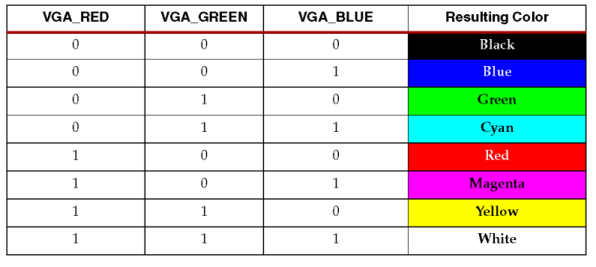
Figure: RGB Code Table.
You will output these signals directly out of your high level component
which encapsulates your VGA driver and the bars components. With
RGB, we can have at most 8 colored states so divide the horizontal
pixels into 8 parts from left to right with each color section.
Each color section will have a unique RGB setting corresponding
to the horizontal count range. As a reminder, you should only write
the color value when you are within the valid hcount and vcount
range, otherwise you might get a flickering VGA screen (this means
the VGA pixel mist be "black" during the other regions).
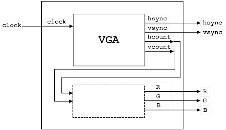
Figure: TV bars Block Diagram
Inputs: Clock, Reset, Enable
Outputs: Hsync, Vsync, R, G, B
Note: Do not forget, the VGA is based on a 25mhz, so once
again use the Xilinx DCM or Clock Generator component!
Download your design to the board, taking into account the proper
pins for the onboard clock, and VGA (see the user guide).
Part 3 - BRAM Image
Now that you have some basic knowledge of how the VGA component
works and how to use the hcount and vcount signals to our advantage,
lets make a slightly more complicated design. In this part, you
will a Block RAM (BRAM) to draw a image of your choosing. BRAMs
are configurable memory unit that has configurable depth, width,
latency and ports. We will use the BRAM to store an image of your
choosing. The image can be small, maybe about 100 pixels wide and
in height, although you are free to do whatever you want. Google
Images has lots of pictures if you search and do not use colored
bars, noise, or other non-trivial designs...
A nice way to access the memory is take advantage of the hcount
and vcount signals generated by the VGA component, and concatenate
the two signals into one BRAM address which will address the BRAM
with your name in it. For example, if you wanted to put your image
in the top left corner, and you concatenate hcount and vcount together,
you will address the 0th element in memory, which is
exactly what you wanted. Placing your image in the middle of the
screen works the same way, but you might have to do a few other
computations to generate your address. Think about it a bit before
doing anything else. You can use a sample
memory.vhdl or generate your own
BRAM, just select RAMB16_S1 in the IPCore Generator. Also here is
an example of a checkerboard (checkerboard.vhdl).
Note: It might be to your advantage to write a small script
that converts a simple image you get off the internet to the BRAM
format. Then, you can just plug the BRAM contents into your code
and it should work just fine Perl and Python should have some utilities
to read an image, although you are free to use whatever you want.
Recommended C++ program steps:
1. EasyBMP to data
structure then to .coe format
Read the images color channels using the EasyBMP library and put
values into a data structure. The libraries, documentation, and
a example for EasyBMP is provided below.
EasyBMP_1.06.zip
EasyBMP_Documentation_1.06.00.zip
BMP_Image_Parce_to_RGB.cpp
Xilinx provides a library of pre-made components for us to use;
one such component is the Block RAM. Add a BRAM to your design by
selecting New Source, then IP (Core Generator). Select Memories>RAMS
& ROMS>Block RAM Generator. A configuration manager will open to
allow you to customize the BRAM component. Make sure to select 'single
port ROM' as the memory type. You should configure the depth (number
of addresses) and width (number of RGB value bits) appropriately
for the image size and quality that you want.
Inside of the BRAM configuration wizard you must specify a .coe
file to load the memory with. The .coe files specifies the contents
of your memory (your image). It would be helpful to write yourself
a script program that converts a bitmap image file into a .coe file.
A nice bitmap (BMP)
image processing library for C++ is EasyBMP.
An example .coe file for a 2x2 pixel image would resemble the test
below. The first two lines must be copied exactly. The following
lines specify the value of each address in numerical order starting
with 0.
Memory_initialization_radix=2;
Memory_initialization_vector=
00,
00,
01,
01; |
Once you have configured the BRAM, you can view the instantiation
template in ISE to add the component to your top-level design. The
BRAM should have 3 ports if correctly generated: clock, input address,
and data output. The functionality of the BRAM is the data output
will reflect the value found at the address input after 1 clock
cycle latency.
Extra Credit


Make an animated character by storing 2 or more images
and alternating between them. For even more bonus credit, make you
character move across the screen (simulate walking or running, for
example).
OR
Make a screen saver, where your image moves completely around the
screen in a bouncing manner. For even more bonus credit, have several
images bouncing off each other and the screen boundaries.
OR
Make the character change directions as the bounce from the boundaries.
You can do this by reversing the order you read the image. For even
more bonus credit, make two or more characters do this across the
screen taking into account when the collide with each other.
OR
Become more creative and attempt to use this
sync_ram.vhdl with some of the
ideas above!
Here is the test bench sync_ramtb.vhdl
|