Lab 3 : Advanced FSMs
Part 1 - Serial Communication to the PC
Serial communication is often used either to control or to receive
data from an embedded microprocessor. Serial communication is a
form of I/O in which the bits of a byte begin transferred appear
one after the other in a timed sequence on a single wire. Serial
communication has become the standard for intercomputer communication.
There are many different protocols for serial communication, including
the USB (universal serial bus) protocol. In this lab, you will implement
RS-232, a simple yet important serial protocol scheme still widely
used today. UART stands for Universal Asynchronous Receiver/Transmitter,
meaning a clock signal is not necessary. However, this means that
each communicator must know the speed at which the data streams
through, as well as some scheme to allow the sender to tell the
receiver when the sender is starting a transmission, and when it
is stopping. RS-232 is a communication protocol designed for UART
systems that has a very simple protocol for achieving the start
and stopping conditions in Figure 1.
RS-232 Protocol
The sender strobes a logical high to a receiver until it is
ready to send a byte of data.
The sender sends one start bit at a logical low to the receiver.
The sender then sends the byte of data, one bit at a time.
After one byte of data, the sender sends a stop bit, which is
a logical high.
(Repeat)... if necessary
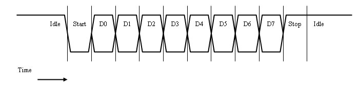
Figure 1: Shows the timing diagram for RS-232 protocol.
The timing diagram labels the logic high step at the beginning as
the "Idle" state. The RS-232 protocol is simply a finite state machine
with the states: IDLE, START, DATA0, DATA1, DATA2, DATA3, DATA4,
DATA5, DATA6, DATA7, STOP.
The rate at which the data is being streamed through is called the
Baud Rate. The baud rate is essentially the rate at which the FPGA
will be transferring bits between communicators. As stated earlier,
both communicators must be in agreement about the baud rate, or
the data received will be garbage.
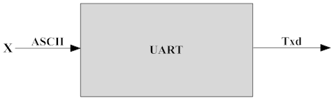
Figure: UART block diagram.
You will only implement a component that transfers data, although
receiver code could easily be extracted.
Entity: uart_transfer
Inputs: Clock, Reset, Enable
Outputs: Txd
Implement the RS-232 protocol, repeatedly sending the letter
'X' in ASCII over and over. The data rate should be at 9600 baud.
Remarks: You might want to consider several options for
implementation of the UART transfer component; there are definitely
several different ways of accomplishing this task.
What about the 9600 baud rate? Well, you know that the Spartan-3E
boards have an onboard 50Mhz clock. How can you use onboard
clock to generate a clock that gives us 9600 bits/second? That's
right! A clock divider/multiplier! Use the provided
clock generator to generate
the baud rate clock. Use the onboard clock for the overall system
calculation and have data ready to be sent when the baud clock
is rising edge. When using the clock generator correctly, the
system should not have clock skew. However, if your system does
have clock skew then use a global clock buffers (BUFG) fix skewed
signal. To use the BUFG "hard" block on the FPGA refer to the
advanced user guide.
Note: The instantiation of BUFG is also in the device
primitive section of the language templates.
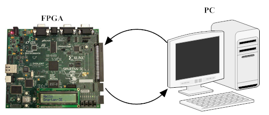
When you have completed your design (simulated and tested),
you are ready to test it by connecting your board to your lab machine,
and communicating with the serial communication program.
- In a Linux terminal type cutecom
- A graphical interface will appear as in figure 2.
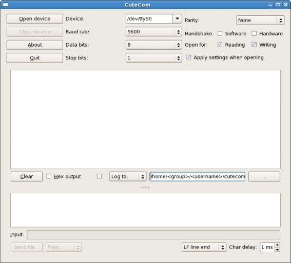
Figure 2: Shows the cutecom graphical setup.
You will need to set up some options for the serial connection,
including Device (/dev/ttyS0) Baud Rate (9600), Data bits (8),
Stop bits (1) Parity (none), Open for (Reading/Writing).
Once set, select the Open device button to activate the
connection.
Download your design to the board, taking into account the proper
pins for the onboard clock, and built-in serial connection (see
the user guide).
Note: Clock is the global clock, Reset is to be switch 0
and Enable is to be switch 1, Txd is on the DCE Female TXD.
Here is a sample bit file: serial_uart.bit
Errors: If you get junk ASCII values on the cutecom then
switch to hex mode. Try to see where the bits of data are miss-aligning
on transmission/receiver ends then correct hardware modules accordingly.
Part 2 - UART Serial Communication "Hello, World"
In previous part, you coupled the letter 'X' right into the UART
transfer component. For a more robust design, you would not want
to have an 'X' directly in the component; rather have the UART component
be attached to some decoder, memory, or register file. Using the
decoder, memory, or register file will allow the UART component
to fetch each letter one at a time, allowing the UART for more than
one function. Using the more robust design will allow the display
of larger messages by simple memory fetches.
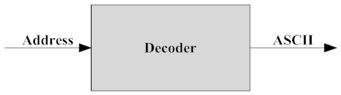
Figure: Decoder block diagram.
- Design a simple decoder, memory, or register file component
that takes as input an address vector and will output a 8-bit
vector, which will correspond to a letter in the alphabet. For
instance, if you designed a decoder with a 5-bit std_logic_vector,
you could encode the 26 letter alphabet, with a few extra characters
to spare.
- Interface your UART transfer
component with your new decoder, memory, or register file component,
and together with some new logic, output to the terminal "Hello
World!", or a longer message of your choosing (do not use
profanity or derogatory language).
Part 3 - UART I/O
Modify your UART transfer to become a more powerful UART. Meaning,
you will need to implement the receiver end. The receiver is similar
to the transfer module, only now you have to wait until you see
a start bit, and then recording the data coming in (Note:
the data will be coming on the Rxd signal line). The
serial communication program does not have built-in echo capabilities,
so you will have to receive the transmission on the FPGA and send
it back to the serial communication program. Making this functionality
allows your message to show up on the serial communication program.
High level functionality description: When you type in the
input component of the cutecom terminal the data will flow from
the PC to the FPGA through the Rxd. The modules you created will
then parse the data from the ASCII transmitted codes and resend
the data to the Txd through your RS-232 module. From here the test
should reappear onto the cutecom read terminal, confirming what
you typed.
Introduction to PS2
You learned how to use the RS-232 protocol to exchange information
to and from two computers. Now you will examine and implement the
PS/2 protocol by designing a PS/2 keyboard interface. Modern keyboards
communicate over a USB or PS2 port. We will focus on the PS2 port.
Each key on a keyboard has a corresponding scan code. While most
keys have a single, 8-bit scan code, some (such as the arrow keys)
have 16-bit scan codes. The scan codes for the left side of a keyboard
are displayed Figure 3.
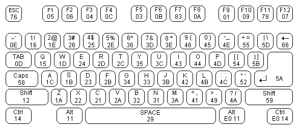
Figure 3: Shows the keyboard code layout.
(From:
Beyond Logic)
Communication between the PC and the keyboard occurs over two 1-bit
lines, which we will refer to as ps2clock and ps2data. For simplicity,
we will only discuss communication from the keyboard to the PC,
though bidirectional communication is possible. Initially, ps2clock
and ps2data are logical high. When the keyboard wishes to send a
scan code (to indicate that a key has been pressed, for example),
the keyboard brings ps2data low to signify a start bit and begins
cycling ps2clock. On subsequent falling edges of ps2clock, ps2data
will hold one of eight bits of the scan code being sent, least significant
bit first. After the scan code has been sent, an odd parity bit
is sent (odd parity means that the number of 1s in the scan code,
including the parity bit, is odd) for error checking. Finally, both
ps2clock and ps2data are brought back to high. The process is summarized
in the following diagram:
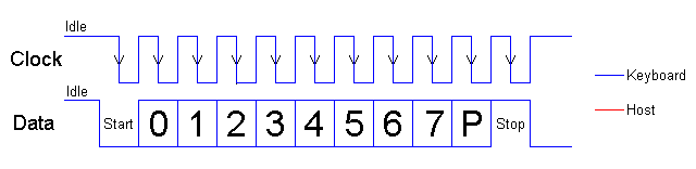
Figure 4: Shows scan code timing diagram.
(From:
Beyond Logic)
As an example, let's assume that the spacebar was pressed. The scan
code for the spacebar is 0x29, which is "00101001" with an odd parity
bit of "0". When a key is released, the keyboard sends the scan
code "0xF0" followed by the scan code of the key that was released.
If a key is held down, the keyboard will send that key's scan code
approximately every 100ms.
Part 4 - PS2 Interface
Create a folder for your lab work and download the following files:
ps2_keyboard.vhdl and
filter.vhdl
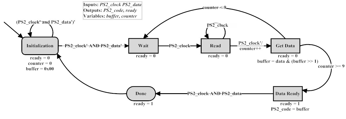
Figure 5: High level FSM for the PS2 Keyboard component.
The ps2_keyboard.vhdl has a component already instantiated
(described in filter.vhdl) that seems to have been coded without
being properly commented. What is the purpose of that code? Is it
even needed? Decipher what it is doing, as it may help you in the
design of how to capture the input coming from the keyboard.
In testing, the output of your keyboard interface will be connected
to the 8 LED lights onboard the Spartan-3E (Note: this does
not take into account the 9th parity bit). For example, if the spacebar
is pressed, "0029" in binary, or "00101001" should be displayed.
Hint: If you have not noticed by now,
this
is a very good reference.
We've written a testbench that you can use to test your design (if
you prefer to work in the simulation environment) which is available
here: ps2_keyboard_tb.vhdl.
The testbench will simulate sending the scan code for the spacebar.
Note: If you use the testbench, you must modify
ps2_keyboard entity to provide an output.
- Implement the rest of the PS/2 interface, so the correct
scan code shows up on the LEDs.
- Download the code to Spartan-3E board.
Inputs: Clock, Reset, Enable, Ps2_Clock, Ps2_data
Outputs: Txd, Output (simulation only)
Download your design to the board, taking into account the proper
pin connections (see the user guide).
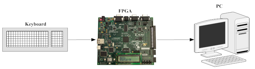
Part 5 - PS2 and UART
We will now interface the PS/2 keyboard component to the UART you
designed. The final system will allow you to type into a keyboard
connected to the FPGA, and have its output directed to the serial
communication program screen, via your UART transfer component.
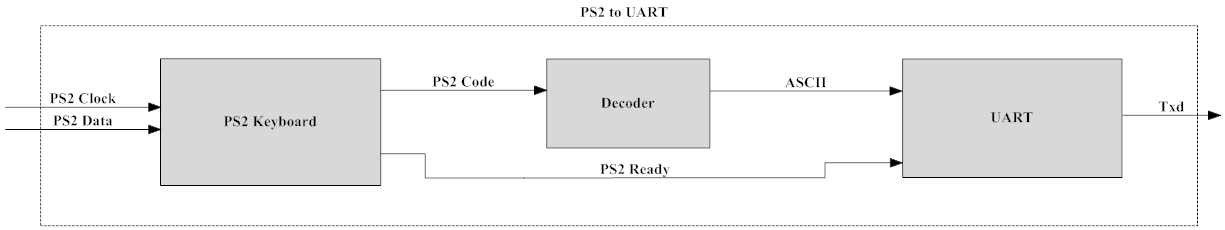
Figure 6: High Level PS2 to UART block diagram.
Of course, at the stage our components are in right now, we can't
simply connect them together and expect everything to work correctly.
Your uart_transfer component repeatedly typed the
same message over and over again, with no intention of stopping.
Now you may need to add an extra input to the uart_transfer.
There may be other signals you need to add, the overall design of
the system is up to you though. You will also need a component that
will translate the scan code generated by the ps2_keyboard
into the ASCII equivalent for the uart_transfer.
You may do this any way you like, although the simple decoder, memory,
or register file you designed in the previous part will probably
work as a good template.
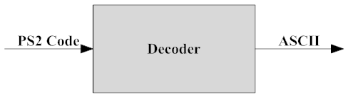
Figure: PS2 Decoder block diagram.
- Implement the interface between the PS/2 keyboard component
and your UART transfer component.
- Because there a lot of keys on the keyboard, and adding
the
shift essentially doubles that amount, we ask
that you only have support for the lower case letters and the
space bar.
Extra Credit
In the previous, the character(s) you typed would show up on the
output multiple times. Fix it so a character will only show up once,
unless you hold the key down for over a half second, which then
outputs the same character every tenth of a second while the key
is held.
|