|
Joseph
Tarango |
|
Home |
Introduction to FPGAsWhat is an FPGA?A field-programmable gate array (FPGA) is a fine-grained reconfigurable fabric used in several applications such as integrated circuit testing and software acceleration. The fabric is made of several components including: logic blocks, I/O blocks, routing channels (interconnect), and several "hard" blocks. Logic blocks are cells consisting of lookup tables (LUTs), these LUTs operate as an array with direct one-to-one mapping (injective function) from its inputs to outputs. I/O pads are used to buffer input and output data. Routing channels or interconnect are the connections for the data to flow to all of the blocks within the FPGA. Depending on the FPGA vendor, there can exist several "hard" blocks, which are integrated circuits to speed-up special operations such as adders, multipliers, random access memory, etc. The details for the architecture are quite extensive and can be found in several academic and industrial published papers.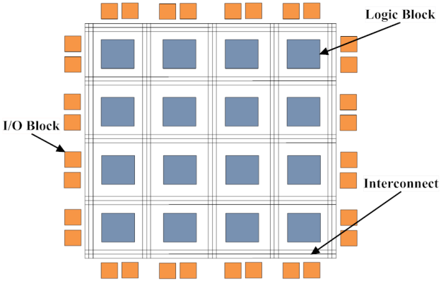 Figure 1: Shows the generic fabric of FPGAs. The interesting feature of FPGAs is that we can change the connections of the fabric statically or on-the-fly depending on the computation. To define such a fabric, the user provides a hardware description or a schematic design. To work with large structures, a hardware description language (HDL) is preferred; there exists several HDLs and in this class we will use VHDL. The tool-chain to compile the HDL onto the fabric happens in several steps. These steps are logical synthesis, translation, technology mapping, and placement and routing. Logical synthesis is the process of abstracting the HDL in terms of logical gates; an example is Berkeley's ABC. The logical synthesis process uses algorithms and data structures to reduce and optimize the logical gates for several design strategies, including area and delay. When the logical synthesis process is complete, the data is sent to translation. The translation is the first step in the implementation process, where all inputs, outputs, and design constraints are put into a logical structure to be used for the target fabric; translation then sends the data to technology mapping. Technology mapping takes the logical structure and creates lower-level primitives for placement and routing; and example is VPR. Placement and routing then takes the primitives and places these on the specific fabric with all logical structure and interconnect. Finally, a bitstream is then created to upload to the specific FPGA. With the bitstream, the design can be uploaded to the FPGA for physical operation. |