Lab 2 : FSMs
Part 1 - Scrolling LED
In this section, you will create a simple light show with the Spartan
3E board. The LEDs will light up from left to right, then scroll
back with a 500 ms delay. To implement this behavior you will need
a finite state machine.
The clock on the Spartan-3E runs at 50 Mhz, so that means there
are are 50,000,000 cycles for every second. To get about a 500 ms
delay you will need to count 25*106 cycles. To calculate
the number of bits you will need for a counter you will need to
find a bit range just above 25*106 (Doing some simple
math... 225=33,554,432), therefore we will need a 25
bit counter. If you happened use a generic template with a generate
statement in the last lab just change your generic parameter, however
for everyone else just make a new 25 bit counter.
Your finite state machine should have at most 1 plus the number
of LEDs used, anymore and you are wasting hardware space!
Inputs: Clock, Reset
Outputs: Leds
To map the inputs and outputs to a physical pins on the FPGA, refer
to the Spartan 3E user manual. Use the "South Button" to reset the
FSM, LEDs<0> to be Led0, Leds<1> to be Led1 and so on...
Part 2 - Greatest Common Divisor
Greatest common divisor (GCD) of two integers is the largest positive
integer that divides both numbers without remainder.
Greatest common divisors can in principle be computed by repeatedly
subtracting the larger integer by the smaller integer until two
integers are the same. At that point the value of the integers is
the GCD of the two original integers. Using 24 and 15 as an example.
Initially in (24, 15), 24 is larger so it is replaced by 24 - 15
= 9. Now we have (9, 15), 15 is replaced by 15 - 9 = 6. In (9, 6),
9 is replaced by 9 - 6 = 3. In (3, 6), 6 is replaced by 6 - 3 =
3. Since both integers in (3, 3) are the same, 3 is the GCD of the
integers 24 and 15.
The first step to write it in VHDL is to draw a complete FSM. All
complexity of writing the VHDL should be coming up with a correct
FSM. With the FSM, you just need to use VHDL to describe it.
The FSM of GCD can be defined as follows. You can test it by steping
through the FSM with the above example.
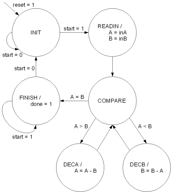
Figure: GCD FSM
The second step is to start with a VHDL component and decide inputs
and outputs. Based on the FSM, we have 3 inputs (inA, inB,
start), 2 inputs for sequential elements (clock,
reset), and 2 outputs (O, done).
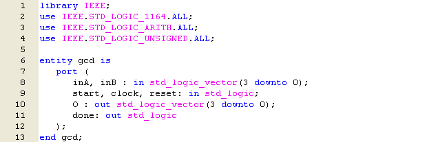
Then we need to determine all the registers in the FSM. State is
always a register in FSM. In the FSM, we also use A and B to keep
values across state, so they are also registers. For each register,
we have to declare *2* signals, one for register output and the
other for register input. We declare them in pairs. In the "process"-statement
that declares registers, we use the register template and simply
replace the names of the register inputs and outputs into the template.
Here we use a single "process"-statement to declare all registers
at onces.
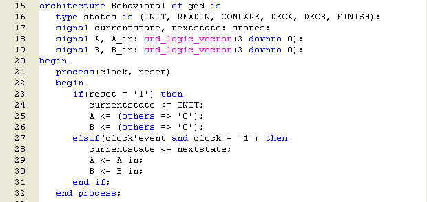
The next "process"-statement defines the transitions of the FSM.
Note the sensitivity list contains all signals that are
used as input in the "process"-statement.
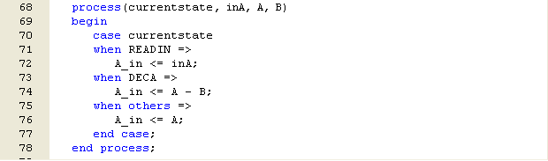
Next we have a "process"-statement that calculates the register
input of A (A_in). In the FSM,
A only changes in two states: READIN and
DECA. For the remaining states, A remains the same.
** Note that in the following "process"-statement, the register
outputs (currentstate, A, B) are always on the
right hand side and register inputs (nextstate,
A_in, B_in) are always on the left hand side.
** This is because the register outputs are the inputs of the combinational
logic and register inputs are the outputs of the combinational logic.
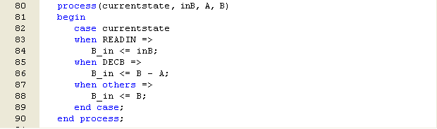
Similarly, a "process"-statement for B.
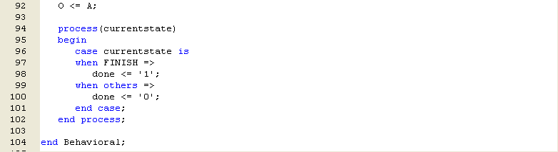
Last, we define the output. Output O is simply the value in one
of the registers. Both A and B have the same value at the end when
it is done. And the done signal is high when it
is done.
Use the following testbench to verify that your component behaves
properly: gcd_tb.vhdl
Part 3 - Fibonacci Number Calculator
Fibonacci numbers are very old sequence of numbers related to self-organized
process made famous by Da Vinci Code. Mathematically, we can define
the n-th Fibonacci number as the sum of the (n-1)-th and (n-2)-th.
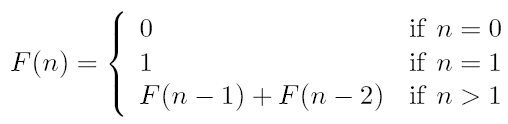
The first 10 Fibonacci numbers are 0, 1, 1, 2, 3, 5, 8, 13, 21,
34. In this lab exercise, you will design a sequential circuit which
computes the n-th Fibonacci number using VHDL.
Specification
- Upon reset, the circuit wait for a
start signal then read in the value of
n from input (4-bit).
- Then the circuit starts to compute iteratively the n-th
Fibonacci number.
- When the number is computed, output (8-bit)
contains the n-th Fibonacci number and done
is high.
- The circuit waits until start is low and
wait for a new computation.
Recommended design Flow
- Design the finite state machines to carry out the computation.
Draw the FSM on a piece of paper!
- Account for the basic logic components you need to compute
the Fibonacci numbers, for instance, registers, etc.
- Implement the FSM in VHDL.
- Simulate your code and make sure it behaves correctly.
You also need to write your own testbench to test your
Fibonacci Number Calculator. There are plenty of examples you have
used. Test your Fibonacci Number Calculator with at least 10 different
test cases.
After adequate testing, now put the design on the FPGA. Remember
the clock on the Spartan-3E runs at 50 Mhz so use a counter to only
output every second.
In your .ucf file:
- Use the LEDs to display the Fibonacci number
- Use the Switches for inputs
- Use the north button to start
- Use the south button to reset
Part 4 - Pattern Matching
A classic application of FSM is pattern matching. It is particularly
useful in applications such as virus detection to detect virus on
a stream of bits (0s and 1s) when it passes through a router. For
example, you get a stream of bits: 001101010111001110111.
And you try to find the string 00111, which appear
in the underlined substring 001101010111001110111.
The FSM to match a pattern from a stream can be modeled in the following
way:
- First make a straight line of states assuming the input
stream is the pattern, and name each state the current matching
stream as follows:
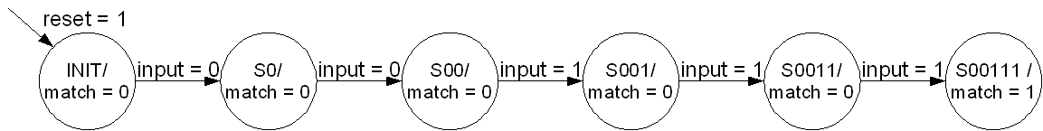
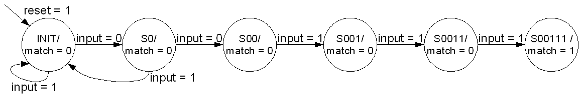
- Since the input bit in each state can be either
0 or 1, you have to fill in an edge
for the other input that does not match the pattern for every
state. For example, if a 1 is input in the
INIT state, it does not start matching the
pattern, so it goes to the INIT state.
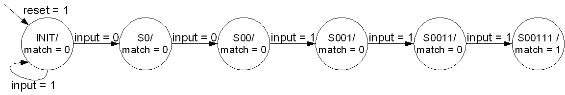
- In the S0 state, if a 1
is input, it does not start matching the pattern, so again it
goes back to the INIT state.
- In the S00 state, if a 0
is input, we have bits 000 as last 3 bit inputs.
The end of 000 is matching the beginning
of the pattern, so it goes to the S00 state.
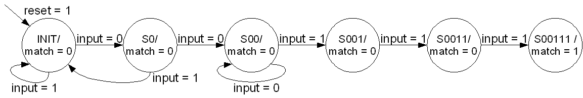
- Continue filling in the edges. As a result, you will have
the following FSM:
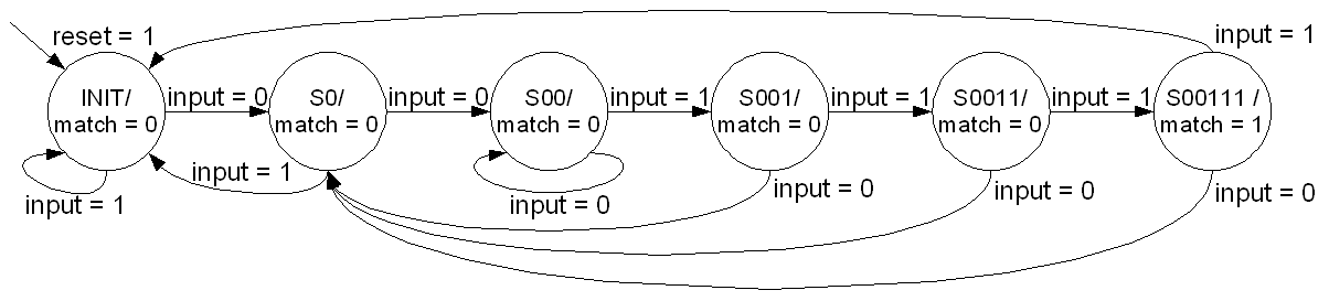
The entity of the FSM should be same as follows:
Entity Name: matchfsm
Inputs: clock, reset, input
Outputs: match
Implement the FSM and test it with
matchfsm_tb.vhdl. In
addition to the above pattern, we would also look for the pattern
01001 (another virus, for example), which the
01 at the end can be the beginning of the second
pattern. Although it is possible to write one FSM to match both
patterns, it is easier to have two FSMs, one for each pattern. Following
the above steps, Draw the FSM on a piece of paper!
Implement the FSM as a separate module / entity and test it with
a testbench. You can use the testbench above for reference.
Now write a top level module that includes the two modules / entities
above. It should have the same input / output pins as the above
components, and the result (match) pin output should
be OR together so that the match is
high when the stream matches either one of the pattern.
Again, write your own testbench.
Extra Credit
Implement a leading zeros detector for a 32-bit binary number. A
leading zeros detector takes in a binary value and counts the number
of consecutive zeros. Once this chain is broken the circuit outputs
the number of leading zeros found in binary. I.E. input = "00001011",
output = "0100".
OR
For triple extra credit, read this academic paper and implement
the leading zeros detector structurally.
Oklobdzija, V.G.; , "An algorithmic and novel design of a leading
zero detector circuit: comparison with logic synthesis," Very
Large Scale Integration (VLSI) Systems, IEEE Transactions on
, vol.2, no.1, pp.124-128, March 1994 doi: 10.1109/92.273153
URL:
http://ieeexplore.ieee.org/stamp/stamp.jsp?tp=&arnumber=273153&isnumber=6757
When completed, verify your design with your own testbench for nearly
all possible cases!
|