Lab 1 : Basic Components
Introduction
Before beginning these exercises read the webpages: Intro to FPGAs,
Basics of VHDL, Intro to Xilinx, and Turnin.
For this lab you will create Parts 1-8, in VHDL with the specified inputs
and outputs then synthesize and test these components with the given
testbenches. If you are struggling to remember the logic behind the
parts in the lab exercises then refer to previous computer science books.
Example Code
Testbenchs
Note: Only for this lab will testbenches be provided. It
is your job as a student to correctly test assignments before turning
them in. You should review the provided code and understand how
to make your own test benches.
In Parts 1-5 you will be creating combinational circuits, where the
output depends on the current values of the inputs. The entities are
to be declared as strictly structural and none of these entities should
not have a processes statement in them.
In contrast, Parts 6-8 are sequential circuits, where the output depends
on both it current input and its previous inputs. In other words, a
sequential circuit maintains a state and its output depends on its current
input and the state the circuit is in. All of the circuits are to be
synchronous, meaning all of the changes happen at the rising edge of
the clock cycle; the reasoning for this is buried in the Xilinx documentation
relating to gated clocks. Gated clocks can cause clock skew, where all
of the synchronized registers are not guaranteed to meet timing requirements.
Other benefits exist from creating strictly synchronous designs, such
as better logic reduction in synthesis, retiming in circuits for faster
clocking, and better timing for deep pipelined circuits. All of these
positive attributes relate to the fundamental architecture of the FPGA
fabric, which is not discusses in this class.Part 1 - Bitwise NOT
(32-bit)
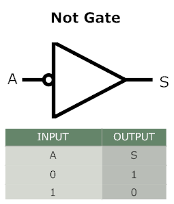
Figure: NOT gate
File Name: lab1_part1.vhdl
Entity Name: not32
Inputs: A
Outputs: S
Logic: S = A'
Description: Create a 32-bit bitwise NOT logical operator.
The architecture is to be defined structurally. A is a binary value.
Part 2 - Bitwise AND (32-bit)
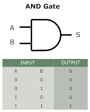
Figure: AND gate
File Name: lab1_part2.vhdl
Entity Name: and32
Inputs: A, B
Outputs: S
Logic: S = A + B
Description: Create a 32-bit bitwise AND logical operator.
The architecture is to be defined structurally. A and B are binary
values.
Part 3 - Multiplexer (32 bit) with 2-bit select
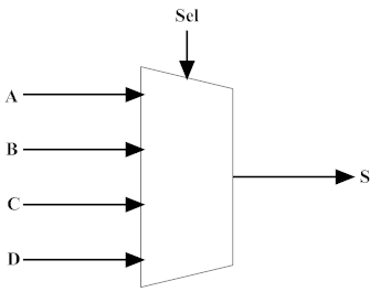
Figure: Mux block
File Name: lab1_part3.vhdl
Entity Name: mux4
Inputs: A, B, C, D, Sel
Outputs: S
Signal Description: When Sel is zero, S is A. When Sel is
one, S is B. When Sel is two, S is C. When Sel is three, S is D.
Description: Within a architecture structurally define a
multiplexer.
Part 4 - Shift Left (32-bit) with no wrapping
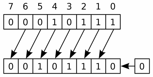
Figure: High level shift left
File Name: lab1_part4.vhdl
Entity Name: shift32
Inputs: A, B
Outputs: S
Description: Create a shift operator, where A shifted left
by B with zeros in place of every shift. The architecture is to
be defined structurally. A and B are binary values.
IE: A = binary "11110001", B = binary "00000011", S = binary
"1000100".
Part 5 - Adder (32-bit)
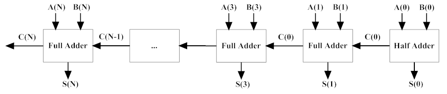
Figure: Adder
File Name: lab1_part5.vhdl
Entity name: adder32
Inputs: A, B
Outputs: S, Overflow
Mathematical: S = A + B
Directions: Structurally define half adder and full adder
components to create a ripple carry adder. The ripple carry adder
is defined structurally within the architecture. A and B are binary
values.
Note: When, adding two large numbers an overflow can occur.
Overflow can be checked the last carry out bit!
Half Adder
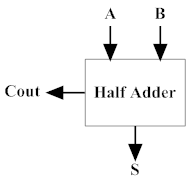
Figure: Half Adder
File Name: lab1_part5a.vhdl
Entity Name: halfadder
Inputs: a, b
Outputs: s, cout
Logic: s = a xor b, cout = a.b
Full Adder
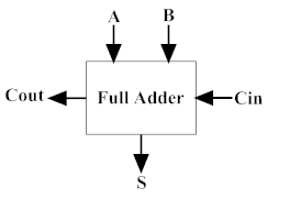
Figure: Full Adder
File Name: lab1_part5b.vhdl
Entity Name: fulladder
Inputs: a, b, cin
Outputs: s, cout
Logic: s = a xor b xor cin, cout = (a.b)
+ (a.cin) + (b.cin)
Hint: Define the adder units unit, then use a generate statement
to define the number of bits. If a generic is used in the entity
description, then portability across systems will be easy.
Part 6 - Synchronous Register (32-bit)
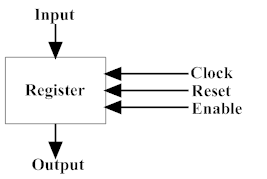
Figure: Single Register
A register is a basic storage element that stores a bit or multiple
bits. Registers are typically composed of multiple D flip-flops.
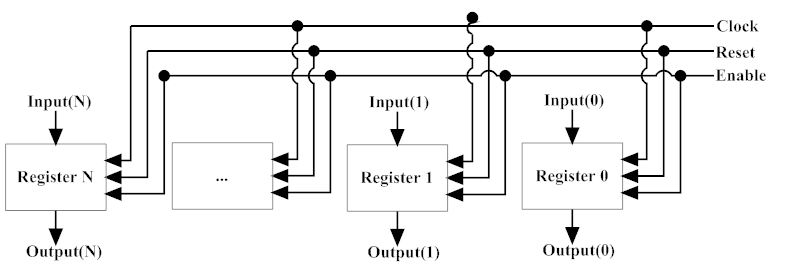
Figure: Register of N bits
File Name: lab1_part6.vhdl
Entity Name: sreg32
Inputs: Clock, Reset, Load, Input
Outputs: Output
Signal Directions: If Reset is high, then the Output is zero.
If Reset is low, and Load are low, then Output keeps previous
Input. If the Load is high, and Reset is low, then input is assigned
to Output.
Description: Create a 32-bit wide register. The register
should operate as a standard synchronous flip-flop, meaning the
reset happens at the rising edge of the clock.
What does the rising edge of the clock mean? The rising edge
of a signal is when the signal makes the transition from low to
high. In VHDL, we describe this action by "clock'event and clock
= 1", where the clock is the global clock of the system.
Hint: Define a register unit, then use a generate statement
to define the number of bits. However, if a generic is used in the
entity description, then portability across systems will be easy.
Part 7 - Synchronous Counter (32-bit)
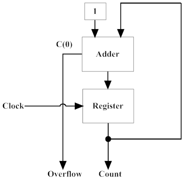
Figure: Counter
As an engineer you will be faced with choices, that have trade-offs.
For your synchronous counter, you can either: use the previous adder
and register to create a counter OR define the counter as a behavior,
the choice is yours!
File Name: lab1_part7.vhdl
Entity Name: scounter32
Inputs: Clock, Reset, Enable
Outputs: Count, Overflow
Signal Description: If Reset is high, then Count is zero.
If Reset low, then Count keeps previous Count. If Enable is high,
then Count gets previous Count's value plus one. If previous Count
is max binary value, then Overflow is high. If previous Count is
not max binary value, then Overflow is low.
Description: The counter can be defined in the architecture
either structurally or behaviorally, but remember the design is
synchronous! Using the adder and/or register component previously
made is recommended!
Hint: Use a generic in the entity description, then portability
across systems will be easy.
Part 8 - Synchronous Finite State Machine
At this point, you have created a simple sequential elements (register
and counter). Now you will put those concepts to use in developing
a circuit that implements a finite state machine (FSM) or deterministic
finite automata (DFA).
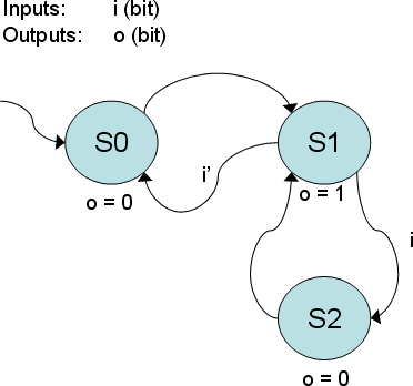
Figure: Sample FSM
A straight forward way to write this in VHDL using a Mealy or Moore
model. A simple reminder differences of the models is a Moore model
outputs in the state, where a Mealy model outputs on the transistion.
For both of these models, it is implied that the transistions have
a clock tick. An overview in performance shows a Moore model performs
better for FPGAs because one-hot encoded state machines have little
to no decoding, however if a binary encoded state mchine is used
then a Mealy model performs better. Knowing which model to use based
on the state machine is not always trivial, therefore, we will use
a Moore Model.
The model can be described a register, transition, and an output
process. Transistion and output are both combinational and the register
process is the sequential memory unit.
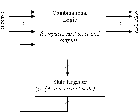
Figure: Synchronous Model
The three process model shown below is a standard way of modeling
a FSM in VHDL. Although there are methods to combine these processes
into one, this model is simpler to understand and debug; if there
should be a logic error in the code.
Note: there are three processes within the FSM architecture,
one process with the label state_register, one process with the
label transition_logic, and one process with the label output_logic.
These processes directly correspond to the FSM diagram above. The
state_register is responsible for reset and loading the value of
the state that it receives from the transition_logic. The transition_logic
is responsible for evaluating the current state to determine the
next state. Lastly, the output_logic sets output based on the current
state.
|
entity
fsm
is
port
(
clock:
in
std_logic;
reset:
in
std_logic;
i:
in
std_logic;
o:
out
std_logic
);
end
fsm;
architecture
arch
of
fsm
is
type
states
is
(S0,
S1,
S2);
signal
currentstate,
nextstate:
states;
begin
-- "state_register" is just a descriptive label we choose.
-- Look carefully at the logic here!
-- On the *rising* edge of the clock,
-- If reset is high, we change the currentstate to S0
-- (look at the FSM to see why S0 was chosen).
-- Otherwise, currentstate gets the value of nextstate.
state_register:
process(reset,
clock)
begin
if
(clock
=
'1'
and
clock'event)
then
if
(reset
=
'1')
then
currentstate
<=
S0;
else
currentstate
<=
nextstate;
end
if;
end
if;
end
process;
-- Again, "output_logic" is just a descriptive label we
chose.
-- Look at how each case statement corresponds to the output
-- based on the FSM diagram above!!
output_logic:
process(currentstate)
begin
case
currentstate
is
when
S0
=>
o
<=
'0';
when
S1
=>
o
<=
'1';
when
S2
=>
o
<=
'0';
-- In case of an error, have output zero.
when
others
=>
o
<=
'0';
end
case;
end
process;
-- Lastly, "transition_logic" is another descriptive label
we choose.
-- Look how the transitions in each condition of the case
statement
-- correspond to the FSM diagram above!
transition_logic:
process(currentstate,
i)
begin
case
currentstate
is
when
S0
=>
nextstate
<=
S1;
when
S1
=>
if
(i
=
'0')
then
nextstate
<=
S0;
else
nextstate
<=
S2;
end
if;
when
S2
=>
nextstate
<=
S1;
-- In case of an error or non-existant state shows up on
-- currentstate, revert to the "reset" state, S0
when
others
=>
nextstate
<=
S0;
end
case;
end
process;
end
arch;
|
Here is a layout of the FSM you are to create
example_fsm.vhdl
File Name: lab1_part8.vhdl
Entity Name: syncfsm
Inputs: Clock, Reset, Enable
Outputs: Output, Valid, Increment, Count, Overflow
Description:
Use the counter you made to be a component in the a synchronous
finite state machine and describe the FSM as a behavior.
Finite State Machine
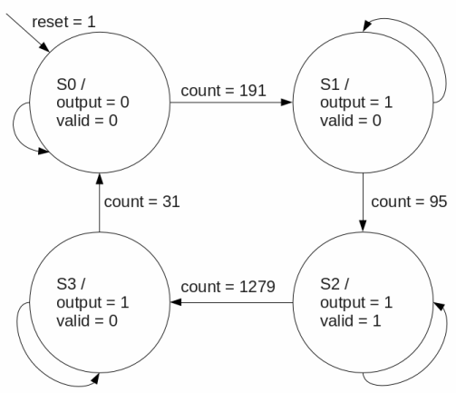
Figure: Partial syncfsm Model
Register
When Reset is high, then in State_0. When Reset is low and
Enable is high, then fsm state is updated with the next
state.
Actions
State_0: Output is low, Valid is low, Count
is Zero, and if Reset is high, then Increment is
high otherwise Increment is low.
State_1: Output is high, Valid is low, Count
is Zero, and if Reset is high, then Increment is
high otherwise Increment is low.
State_2: Output is high, Valid is high, Count
is equal to current counter value, and if Reset
is high, then Increment is high otherwise Increment
is low.
State_3: Output is high, Valid is low, Count
is Zero, and if Reset is high or internal count
is equal to 31(0x0000001F), then Increment is high
otherwise Increment is low.
Transitions
State_0: If the internal count is 191 (0x000000BF),
then next state is State_1, else state is State_0.
State_1: If the internal count is 95 (0x0000005F),
then next state is State_2, else state is State_1.
State_2: If the internal count is 1279 (0x000004FF),
then next state is State_3, else state is State_2.
State 3: If the internal count is 31 (0x0000001F),
then next state is State_0, else state is State_3.
Other Actions
State_0: If (the internal count is 191 (0x000000BF)
and Enable is high) or Reset is high, then the internal
counter is reset.
State_1: If (the internal count is 95 (0x0000005F)
and Enable is high) or Reset is high, then the internal
counter is reset.
State_2: If (the internal count is 1279 (0x000004FF)
and Enable is high) or Reset is high, then the internal
counter is reset.
State 3: If (the internal count is 31 (0x0000001F)and
Enable is high) or Reset is high, then the internal
counter is reset.
Hint: If you make this FSM correctly with generic
parameters for each count check, then you can use this as
a synchronous counter within a VGA driver.
Extra Credit: Make a simple 32-bit Arithmetic and Logic
Unit (ALU) with the NOT, AND, Adder, and Shift Left.
File Name: lab1_ec.vhdl
Entity Name: alu32
Inputs: A, B, Select
Outputs: S, Overflow
Signal Description:
When select is zero, then S is NOT A.
When select is one, then S is A AND B.
When select is two, then S is A shifted left by B.
When select is three, then S is A plus B.
When select is three and adder overflows occurs, then
overflow is high, else low.
Testbench File name: lab1_ec_tb.vhdl
Testbench Entity name: alu32_tb
Description: Create an 32-bit ALU from previous made
components, and test it with your own test bench. You must
prove ALU is completely tested, this includes possible exceptions!
To adequately test the ALU consider the all of the logical
sets, and whether the result can be differentiated from
the input.
NOT := only one test case is necessary, due to direct mapping.
AND := test where the inputs are > {(0,0) , (N,M) , (N,N)}
ADDER := test where the sum is > {(0), (N), (MAX-1), (MAX),
(Overflow)}
SHIFTER := { {Shift by zero}, {Shift by N}, {Shift to MAX-1},
{Shift to MAX or over}}
N, M := independant are integers
MAX := is the maximum integer within the range
|