UCR EE/CS120B: Digital Systems
Lab 1c: Synthesis
I. Introduction
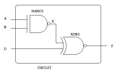
Suppose we want to construct the above circuit. We can describe the
circuit in several ways.
STRUCTURAL DESCRIPTION
If we were to describe the above circuit structurally we would first
have to construct entities which act as AND2 and OR2 gates. Then we
would plug our input values into these entities to get our result. This
was done in the previous lab, the example given was as follows:
...

entity NAND2 is
   port ( input1, input2: in STD_LOGIC;
          output1: out STD_LOGIC
        );
end NAND2;

architecture beh_nand2 of nAND2 is
begin
   output1 <= input1 nand input2;
end beh_nand2;


entity XOR2 is
   port ( input1, input2: in STD_LOGIC;
	  output1: out STD_LOGIC
        );
end XOR2;

architecture beh_xor2 of XOR2 is
begin
   output1 <= input1 xor input2;
end beh_xor2;


entity CIRCUIT is
   port ( a, b, c : in STD_LOGIC;
          f: out STD_LOGIC;
        );
end CIRCUIT;

architecture struct of CIRCUIT is

signal e: STD_LOGIC;

component NAND2
   port ( input1, input2: in STD_LOGIC;
          output1: out STD_LOGIC
        );
end component;

component XOR2
   port ( input1, input2: in STD_LOGIC;
          output1: out STD_LOGIC
        );
end component;

begin
   X1: NAND2 port map(A, B, E);
   X2: XOR2 port map(E, D, F);

end struct;

...
BEHAVIORAL DESCRIPTION
If we were to describe the above circuit behaviorally we would not have
to worry about mimicing the gates. Instead we can describe the result
at a more abstract level which greatly simplifies things as seen below:
...

entity CIRCUIT is
   port ( a, b, d: in STD_LOGIC;
	  f: out STD_LOGIC
        );
end CIRCUIT;

architecture beh of CIRCUIT is
begin
   f <= (a nand b) xor d;
end beh;

...
II. Behavioral Description
Following the steps outlined in lab1B,
write a behavioral vhdl description of the 7 segment decoder and simulate
it.
III. Downloading the schematic design
- You must now modify your schematic by replacing all of your input
and output signals so that they may be mapped to the appropriate
pins on the XS40 board. Replace all of the hirarchy connectors
with "IPADS", which will then be connected to the "IBUF"
symbols
- Now you will have to map the pins on the board to these pads. To
do this, select each pad and double click on it. This should
bring up a window labeled "Symbol Properities." In this window
type "LOC" into the "Name" box and the in the "Description" box
type in the pin number (p80, p81, p10, or p14 depending on the pad),
clicking the "Add" button and then "OK" each time. Do this for
each input pad.
- Follow the same steps for the output pads, but label the
descriptions as follows:
- a - "p19"
- b - "p18"
- c - "p23"
- d - "p20"
- e - "p24"
- f - "p26"
- g - "p25"
- Save this to a different file and return to the "Project Manager"
(the original window that opened). Add this new file to the
project.
- Click on Implementation. This should bring up the "Implement
Design" window. Click "Run" on this window.
- If there are any errors, go back to the schematic and fix them,
otherwise proceed.
- Find the "bit" file that was created and copy it into your home
drive.
- Go to the designated computer and we will download and test
out your design.
IV. Downloading VHDL
- Check out a XS40 board.
- Open up your project under Xilinx. Make sure that the names of
your variables match exactly with those on the web
page (in1, in2, etc.).
- Inside Windows explorer, remove the ".ucf" file in your project
and replace it with lab1c.ucf being sure
to rename it to whatever ".ucf" file you deleted. For example,
if your project was "lab01" you would remove "lab01.ucf" and save
"lab1c.ucf" as "lab01.ucf".
- Now you can run through the Implementation stage and generate
a bit file like before.
- Check out an FPGA from your T.A., open a "Command Prompt"
terminal and cd to "c:\temp\lab2" or wherever your lab is
located.
- Make sure your XS40 board is powered up and connected to the
computer.
- Type "xsload lab2.bit" on the prompt and hit "enter".
Verify your results.
- You must do this for both the structural and the
behavioral description of the 7-segment display converter.