UCR EE/CS120B: Digital Systems


Lab 1B: Intro to FPGA's using VHDL

I. Introduction

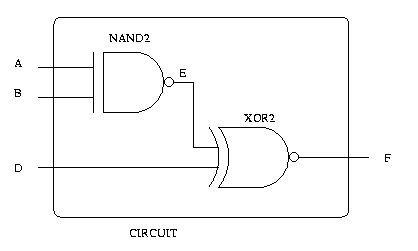
In the previous lab Xilinx was used to draw the circuit by connecting a series of AND gates and OR gates. In this lab you will be taking the previously constructed circuit and describe it in VHDL. To do this you will need to construct entities which mimic the gates used. Then connect the "gates" to construct the 7 segment decoder.


Suppose we want to construct the above circuit.

First we have to construct entities which act as NAND2 and XOR2 gates. Then we would plug our input values into these entities to get our result. An example of this may be as follows:

...

entity NAND2 is
   port ( input1, input2: in STD_LOGIC;
          output1: out STD_LOGIC
        );
end NAND2;

architecture beh_nand2 of NAND2 is
begin
   output1 <= input1 nand input2;
end beh_nand2;


entity XOR2 is
   port ( input1, input2: in STD_LOGIC;
	  output1: out STD_LOGIC
        );
end OR2;

architecture beh_xor2 of XOR2 is
begin
   output1 <= input1 xor input2;
end beh_xor2;


entity CIRCUIT is
   port ( a, b, c : in STD_LOGIC;
          f: out STD_LOGIC;
        );
end CIRCUIT;

architecture struct of CIRCUIT is

signal e: STD_LOGIC;

component NAND2
   port ( input1, input2: in STD_LOGIC;
          output1: out STD_LOGIC
        );
end component;

component XOR2
   port ( input1, input2: in STD_LOGIC;
          output1: out STD_LOGIC
        );
end component;

begin
   X1: NAND2 port map(A, B, E);   
   X2: XOR2 port map(E, D, F);

end struct;

...

II. Implementation

  1. Start up Xilinx and select "Create a New Project" Save it in temp as before. Name it lab2 and select the "HDL" instead of the "Schematic Capture" option.
  2. Click on the little paper icon in the "Design Entry" button. This should bring up the HDL editor. Choose "Empty Design".
  3. Write all of the code to structurally implement the design from the previous lab. The schematic should translate directly into this design only now you should have entities for each component, like an entity for a three input OR gate and others.
  4. Once you have all the program typed in go to "Synthesis" and select "Check Syntax". After ensuring that there are no syntax errors, go back to the "Project Manager".
  5. Select the "Synthesis" step as the next step in the design process. Ensure that the "BCD" entity that you created is selected for the "Top LeveL", and that the Target Device information is as follows: "Family" = XC4000XL, "Device" = 4010XLPC84. Now click on "Run".
  6. Now verify the correctness of your VHDL code, by selecting the "Simulation" button. Add the appropriate signals to your waveform, and their stimuli as you did in the previous laboratory assignment.