Experiments with the Peripheral Virtual Component Interface
Roman L. Lysecky, Frank Vahid*, Tony D. Givargis
Department of Computer Science and Engineering
University of California, Riverside
{rlysecky,
vahid,
givargis}@cs.ucr.edu,
www.cs.ucr.edu/~dalton
*also with the Center for Embedded Computer Systems, UC Irvine
Abstract
The Peripheral Virtual Component Interface, or PVCI, is a standard intended to simplify the interfacing of peripheral cores to on-chip buses in a system-on-a-chip, by standardizing the interface between a core's internals and its bus wrapper. We provide results of experiments intended to determine the power, performance, and size overhead associated with using a PVCI bus wrapper versus using a non-PVCI bus wrapper, and versus using no bus wrapper at all. The results demonstrate that using a bus wrapper may result in only small performance, power and size overhead versus using no wrapper, though even that performance overhead can be reduced or eliminated using pre-fetching. The results also demonstrate that using a PVCI bus wrapper yields no significant additional power, performance or size overhead compared with a non-PVCI bus wrapper.
Keywords
Cores, system-on-a-chip, interfacing, on-chip bus, intellectual property, VCI, bus wrappers.
1. Introduction
Silicon capacity continues to increase faster than the ability for designers to use that silicon, resulting in the well-known productivity gap [1]. Many propose extensive reuse of pre-designed intellectual property cores to reduce this gap [2], where typical cores include microprocessors as well as peripherals like encoders/decoders, bus interfaces, analog-digital converters, serial communication components, etc. In response, several commercial libraries of cores have evolved in recent years (e.g., [3]). Soft cores come in the form of synthesizable code, while hard cores come in the form of technology-specific layouts.
A key aspect of a core’s marketability, soft or hard, is its ability to be easily integrated into a system-on-a-chip (SOC). Unfortunately, standardizing on one or two on-chip SOC buses, which certainly would ease integration, does not appear to be possible because of the diversity of constraints present in embedded systems, as recognized for example by the Virtual Socket Interface Alliance (VSIA) [4]. Thus, to achieve such ease of integration, many have proposed designing cores with their interface behavior implemented in a bus wrapper, separated from the core's internal behavior [4][5][6]. This separation means that changes necessary to adapt a core to a particular bus are limited to the bus wrapper.
In this paper, we analyze the impact of using a bus wrapper on the design metrics of performance, power and size. Furthermore, we analyze the impact on those metrics of using the VSIA interface between a bus wrapper and a peripheral core’s internals versus using a customized interface.
2. PVCI
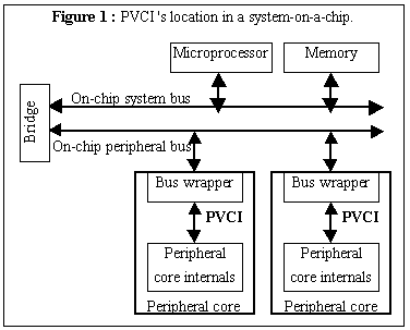
After deciding that a single on-chip bus standard was unlikely, the VSIA developed the Virtual Component Interface (VCI). The VCI is a proposed standard interface between a core’s internals and a core’s bus wrapper, as illust rated in Figure 1. A core with its interface behavior separated into a bus wrapper is believed to be much easier to retarget to different buses than a core whose interface behavior is integrated with its internal behavior. By standardizing the interface between the core's internals and the bus wrapper, retargetting of a core may become easier. Retargetting any core using VCI will involve roughly the same changes to the bus wrapper, since the VCI ensures that the changes are limited to the wrapper and not the internals, and since a bus provider can even provide bus wrapper templates between the bus and the VCI. The VCI is a far simpler protocol than a typical bus protocol, since it is a point-to-point transfer protocol. In contrast, a bus protocol may involve more advanced features, such as arbitration, data multiplexing, pipelining, and so on. Thus, standardizing the VCI is far simpler than standardizing a bus protocol.
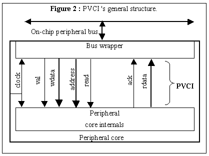
The PVCI is a simplified version of the VCI, specifically intended for peripherals. PVCI cores would reside on a lower-speed peripheral bus as shown in Figure 1, and thus would not need some of the high-speed features of the VCI (e.g., packet chaining). The general structure of the PVCI is shown in Figure 2. It consists of two uni-directional buses. One bus leads from the wrapper to the internals. The wrapper sets the read line to indicate a read or a write, and sets the address lines with a valid address. For a write, it also sets the wdata lines. It asserts the val line to indicate to actually initiate the read or write. The wrapper must hold all these lines constant until the internals assert the ack line. For a write, this means that the internals have captured the write data. For a read, this means that the internals have put the read data on the rdata bus. The transaction is completed on the next rising clock edge. A fast internals module can keep ack asserted continuously to provide for fast transfers, similar in spirit to the synchronous wait protocol [9].
3. Experiments with the ISA bus
We first sought to evaluate the impact of a wrapper and of PVCI when using a widely used peripheral bus. We chose the well-known ISA bus.
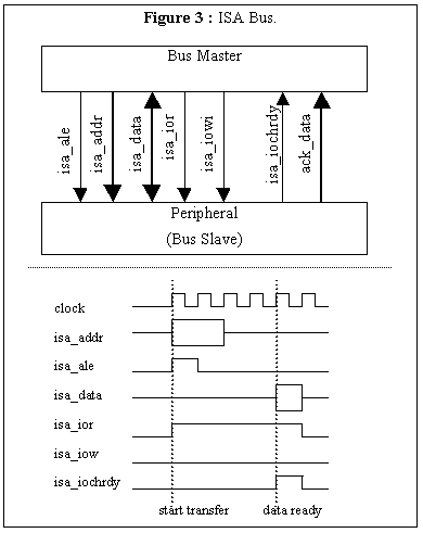
As illustrated in Figure 3 , the ISA bus works as follows. A 23-bit bus, isa_addr, is used for addressing peripheral devices. A peripheral latches the address when the control signal, isa_ale, is asserted. A bi-directional 32-bit bus, isa_data, is used for data transfer to and from peripheral devices. Two control signals, isa_ior and isa_iow, are used to signal a read or write operation. By default all I/O operations take 4 cycles, however, slower peripheral devices can delay the operation as long as they assert a not-ready control signal denoted isa_chrdy. Other ISA control signals such as interrupt-request, byte I/O and DMA control are omitted in this paper.
The example we evaluated was a simple version of a digital camera system, illustrated in Figure 4. The camera system consists of a (simplified) MIPS microprocessor, BIOS, and memory, all on a system bus, with a bridge from the system bus to a peripheral bus (ISA) having a CCD (charge-coupled device) pre-processor and a simple CODEC (compressor/ decompressor). The two-level bus structure is in accord with the hierarchical bus concept described in [2]. The camera is written in register-transfer level synthesizable VHDL, and synthesizes to about 100,000 cells. We used the Synopsys Design Compiler as well as their power analysis tools to evaluate different design metrics. Power and performance were measured for the processing of one frame.
We made changes to the CCD pre-processor and CODEC cores since they represent the peripherals on the peripheral bus. These cores are used heavily while processing a frame. We created three versions of the camera system:
The non-PVCI wrapper version was created for another purpose, well before the PVCI standard was developed and with no knowledge that the version would be used in these experiments. Thus, its structure was developed to be as simple as possible.
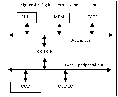
Table 1 summarizes size, performance and power data for the three versions using the ISA bus. Size is reported in equivalent NAND gates, time in nanoseconds, and power in milliwatts. As expected, the integrated version represents the most efficient implementation but at the expense of being harder to retarget to different buses.
The size overhead when using a bus-wrapper (non-PVCI) compared to the integrated version was roughly 1500 gates per core. This overhead comes from extra control and registers. In the integrated version, the core's internals includes control to interface to the ISA bus. In the wrapper version, this control is replaced by control for interfacing to the wrapper, so the size of the core's internals stays the same. However, the wrapper now must implement control for interfacing to the internals, and for interfacing to the ISA bus, representing overhead. The wrapper must also include registers whose contents are copied to/from the internals, representing additional overhead. The reason that the non-PVCI wrapper version shows more size overhead than the PVCI wrapper version is because the non-PVCI version used a single bus for transfers both two and from the core internals, whereas PVCI specifies two separate buses, resulting in less logic but more wires. 1500 gates of size overhead seems quite reasonable, given the continued increase of chips' gate capacities, and given that peripheral cores typically posses 20,000 gates or more [3].
The system power overhead was only about 1%. The extra power comes from having to transfer items twice per access -- on a write, an item must be transferred first from the bus to the wrapper, then from the wrapper to the internals. On a read, an item must be transferred first from the internals to the wrapper, then from the wrapper to the bus. However, the power consumed by the memory, system bus, and processor dominate, so the extra power due to the wrappers is very small -- even though the CCD and CODEC are heavily used when processing a frame.
There was no performance overhead when using a wrapper, because of the fact that ISA uses a minimum of four cycles per access. The extra cycles required for the two transfers per item (as described in the previous paragraph) are performed within those four cycles, and thus no extra cycles were introduced. This lack of performance overhead may not be true for a bus protocol that uses fewer cycles, or a peripheral that requires more cycles to access.
4. Experiments with a custom peripheral bus
The ISA peripheral bus includes a minimum of four cycles, so the use of a wrapper resulted in no performance overhead in our examples. To determine the performance impact for a bus that did not include such a minimum, we modified the system to use a customized peripheral bus. The bus used a two-phase handshake protocol to ensure that the communication was as fast as possible for a given peripheral. Using a wrapper results in a two cycle overhead per read as compared with an integrated core.
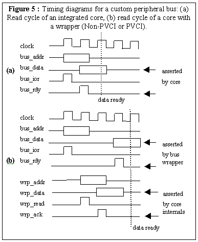
Figure 5(a) illustrates the timing of a read cycle of this custom peripheral bus for an integrated core. The peripheral bus master (in our case, the bridge) places an address on bus_addr and then strobes bus_ior. The peripheral responds by placing data on bus_data and strobing bus_rdy as early as once cycle after receiving the bus_ior strobe. Thus, the total read cycle could be as little as two clock cycles.
Figure 5(b) illustrates the read cycle of the custom bus for a core using a bus wrapper. Since the non-PVCI and PVCI versions have the same timing behavior, they are both represented by a single timing diagram and a set of signals in this figure. After the bus master places the address and strobes bus_ior, the wrapper responds by translating this read request into a read request over the internal bus. This translation involves translating the address to one appropriate for the core and then placing that address on wrp_addr, and then asserting wrp_read. The core's internals responds by placing data on wrp_data and then asserting wrp_ack. The wrapper receives the data, puts it on the peripheral bus, and strobes bus_rdy.
Table 1: Comparison of interface versions using the ISA bus.
| Version | Ex. | Size of Wrapper | Size of Internals | Time for 1 frame | Power for 1 frame |
| Integrated | ccd | 0 | 34367 | 82955 | 7.88 |
| codec | 0 | 1968 | |||
| Non-PVCI wrapper | ccd | 1684 | 34556 | 82955 | 8.11 |
| codec | 1679 | 1904 | |||
| PVCI wrapper | ccd | 1478 | 33978 | 82955 | 7.97 |
| codec | 1474 | 1588 |
Table 2: Comparison of interface versions using a custom bus.
| Version | Ex. | Size of Wrapper | Size of Internals | Time for 1 frame | Power for 1 frame |
| Integrated | ccd | 0 | 34320 | 75175 | 7.90 |
| codec | 0 | 1926 | |||
| Non-PVCI wrapper | ccd | 1661 | 34556 | 79054 | 8.11 |
| codec | 1674 | 1904 | |||
| PVCI wrapper | ccd | 1439 | 33978 | 79054 | 7.98 |
| codec | 1434 | 1588 |
A write cycle need not incur any performance overhead in the wrapper versions. When the bus master sets the addresses and strobes the appropriate ready line, the wrapper can respond immediately by capturing the data and strobing the ready line, just like an integrated core will do. The wrapper can then proceed to write the captured data to the core internals.
Table 2 summarizes size, performance, and power results. Size overhead is comparable to the earlier experiment, roughly 1500 gates. Power overhead is again almost negligible. Unlike the previous experiment, however, there is a performance overhead, though it is quite small, amounting to only about 5%. Furthermore, the overhead was due to the use of a wrapper, which would have occurred whether using PVCI or another other wrapper. In our experiments, the CCD was accessed 256 times per image frame, while the CODEC was accessed a total of 128 times per frame. The MIPS processor executed approximately 5000 instructions per frame.
In earlier works, we demonstrated that in many cases, we can pre-fetch data into register copies added to the wrapper in order to reduce or even eliminate the performance overhead associated with a wrapper [7][8], while still obeying the VCI standard. This approach involves adding register copies from the internals into the wrapper, and adding a pre-fetch control unit into the wrapper. The pre-fetching size overhead ranged from 500-2000 gates. Pre-fetching would eliminate the extra cycles caused by using a bus wrapper in the CCD and CODEC, as those cores fall into categories suitable for pre-fetching described in [7] and [8].
One difference between the non-PVCI and PVCI interface that does not appear in the results is the number of wires internal to the core. The non-PVCI version used a multiplexed bus, and has fewer signals (some PVCI signals were not shown), and thus would have fewer internal wires.
Noting that our CCD and CODEC cores are relatively small and have simple interfaces, it took us 6 designer hours, excluding synthesis and simulation time, to retarget a design from one wrapper to another, e.g., to convert the CCD’s non-PVCI wrapper to a PVCI implementation. Synthes is time for the CCD and CODEC was approximately 1 hour. Simulation time for capturing one image frame was slightly over 10 hours and power analysis was an additional 5 hours. These times were obtained by synthesizing the models down to gates using Synopsys Design Compiler with medium mapping effort, using the lsi_10k library supplied by Synopsys, with no area or delay constraints specified. We used a dual 200 MHz Ultra Sparc II machine to perform both our synthesis and simulation. Synthesis and simulation times were relatively the same between the integrated bus implementations and those using a bus wrapper. We note that peripheral devices that are capable of DMA or burst mode I/O with interrupts will require more time to integrate into a system.
5. Conclusions
Our experiments demonstrated that PVCI results in only minor size, power and performance overhead compared to a non-wrapper peripheral core approach (though pre-fetching can even eliminate the performance overhead), and in almost no overhead compared to an alternative wrapper approach based on a bi-directional bus between a core ’s wrapper and internals. Thus, the retargetabili ty advantages of such a standard seem to come with acceptable penalty.
6. Acknowledgements
This work was supported by the National Science Foundation (grants CCR-9811164 and CCR-9876006) and a Design Automation Conference Graduate Scholarship. The work is part of the Dalton project at UCR (www.cs.ucr.edu/~dalton).
7. References
[1] Semiconductor Industry Association Roadmap 1997, http://notes.sematech.org/ntrs/PublNTRS.nsf.
[2] Virtual Socket Interface Association, Architecture Document, http://www.vsi.org, 1997.
[3] Inventra core library, Mentor Graphics, http://www.mentorg.com/inventra/
[4] Virtual Socket Interface Association, On-Chip Bus Development Working Group, Specification 1 Version 1.0 (OCB 1 1.0), http://www.vsi.org, 1998.
[5] F. Vahid and L. Tauro, An Object-Oriented Communication Library for Hardware-Software Co-Design, International Workshop on Hardware/Software Codesign, pp. 81--86, 1997.
[6] J. Rowson and A. Sangiovanni-Vincentelli, Interface-Based Design, Design Automation Conference, 1997.
[7] R. Lysecky, F. Vahid, T. Givargis, and R. Patel, Pre-fetching for Improved Core Interfacing, International Symposium on System Synthesis, 1999.
[8] R. Lysecky, F. Vahid, and T. D. Givargis, Techniques for Reducing Latency of Core Bus Wrappers, Design, Automation and Test In Europe, 2000.
[9] S. Vercauteren, B. Lin, H. De Man. Constructing Application-Specific Heterogeneous Embedded Architectures from Custom HW/SW Applications. Design Automation Conference, pp. 547-551, 1996.